- 您现在的位置:买卖IC网 > Sheet目录489 > NTK3134NT5G (ON Semiconductor)MOSFET N-CH 20V 750MA SOT-723
�� �
�
�NTK3134N�
�Power� MOSFET�
�20� V,� 890� mA,� Single� N� ?� Channel� with�
�ESD� Protection,� SOT� ?� 723�
�Features�
�?� N� ?� Channel� Switch� with� Low� R� DS(on)�
�?� 44%� Smaller� Footprint� and� 38%� Thinner� than� SC89�
�?� Low� Threshold� Levels� Allowing� 1.5� V� R� DS(on)� Rating�
�?� Operated� at� Low� Logic� Level� Gate� Drive�
�?� These� Devices� are� Pb� ?� Free,� Halogen� Free/BFR� Free� and� are� RoHS�
�Compliant�
�Applications�
�?� Load/Power� Switching�
�?� Interface� Switching�
�?� Logic� Level� Shift�
�?� Battery� Management� for� Ultra� Small� Portable� Electronics�
�V� (BR)DSS�
�20� V�
�http://onsemi.com�
�R� DS(on)� TYP�
�0.20� W� @� 4.5� V�
�0.26� W� @� 2.5� V�
�0.43� W� @� 1.8� V�
�0.56� W� @� 1.5� V�
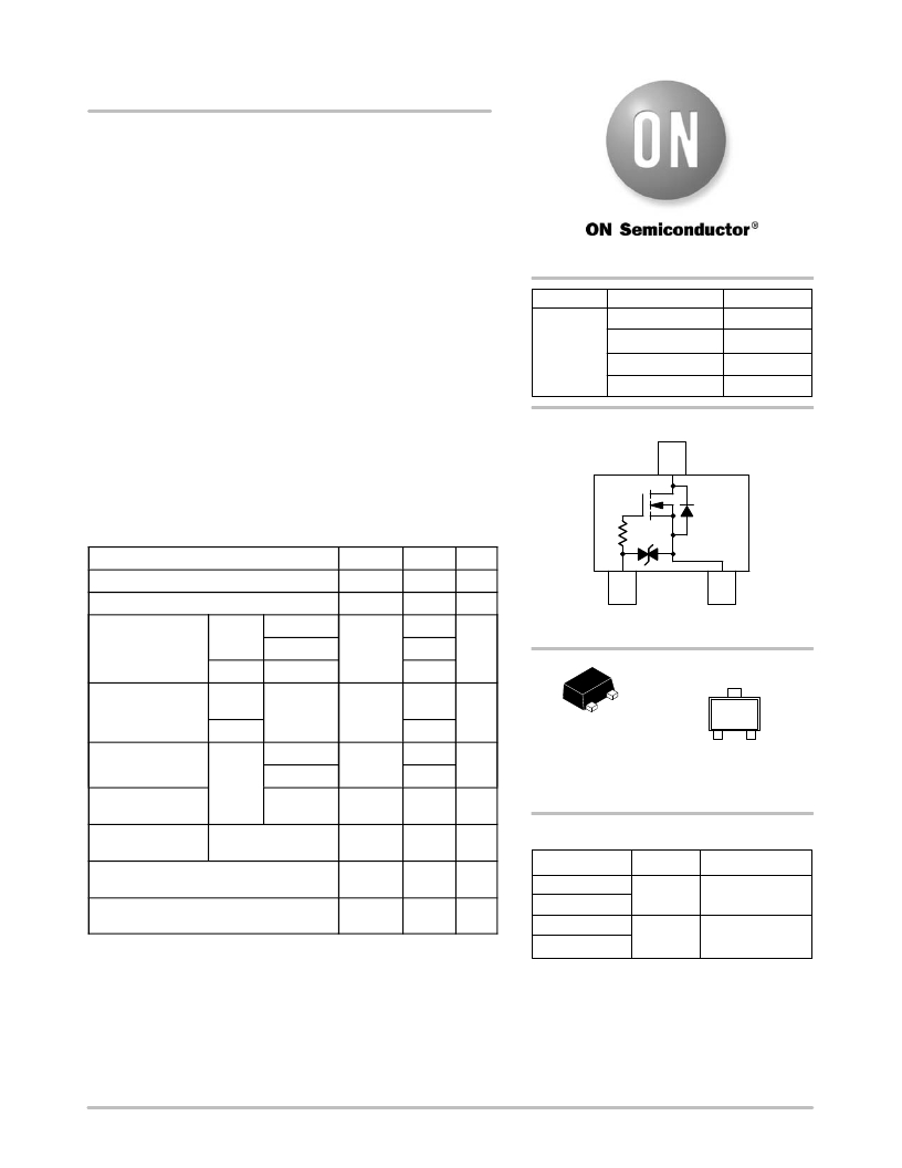
�SOT� ?� 723� (3� ?� LEAD)�
�3�
�I� D� Max�
�890� mA�
�790� mA�
�700� mA�
�200� mA�
�MAXIMUM� RATINGS� (T� J� =� 25� °� C� unless� otherwise� stated)�
�Parameter�
�Symbol�
�Value�
�Unit�
�Drain� ?� to� ?� Source� Voltage�
�Gate� ?� to� ?� Source� Voltage�
�Continuous� Drain� Steady�
�Current� (Note� 1)� State�
�T� A� =� 25� °� C�
�T� A� =� 85� °� C�
�V� DSS�
�V� GS�
�I� D�
�20�
�±� 6�
�890�
�640�
�V�
�V�
�mA�
�1�
�Top� View�
�2�
�1� ?� Gate�
�2� ?� Source�
�3� ?� Drain�
�t� ≤� 5s�
�T� A� =� 25� °� C�
�990�
�MARKING� DIAGRAM�
�Power� Dissipation�
�(Note� 1)�
�Steady�
�State�
�T� A� =� 25� °� C�
�P� D�
�450�
�mW�
�KF� M�
�Continuous� Drain�
�Current� (Note� 2)�
�Power� Dissipation�
�(Note� 2)�
�t� ≤� 5s�
�Steady�
�State�
�T� A� =� 25� °� C�
�T� A� =� 85� °� C�
�T� A� =� 25� °� C�
�I� D�
�P� D�
�550�
�750�
�540�
�310�
�mA�
�mW�
�SOT� ?� 723�
�CASE� 631AA�
�STYLE� 5�
�KF�
�M�
�1�
�=� Specific� Device� Code�
�=� Date� Code�
�NTK3134NT1H�
�NTK3134NT5H�
�Pulsed� Drain� t� p� =� 10� m� s� I� DM� 1.8� A�
�Current�
�Operating� Junction� and� Storage� T� J� ,� T� STG� ?� 55� to� °� C�
�Temperature� 150�
�Lead� Temperature� for� Soldering� Purposes� T� L� 260� °� C�
�(1/8”� from� case� for� 10� s)�
�Stresses� exceeding� Maximum� Ratings� may� damage� the� device.� Maximum�
�Ratings� are� stress� ratings� only.� Functional� operation� above� the� Recommended�
�Operating� Conditions� is� not� implied.� Extended� exposure� to� stresses� above� the�
�Recommended� Operating� Conditions� may� affect� device� reliability.�
�1.� Surface� mounted� on� FR4� board� using� 1� in� sq� pad� size� (Cu� area� =� 1.127� in� sq�
�[1� oz]� including� traces)�
�2.� Surface� mounted� on� FR4� board� using� the� minimum� recommended� pad� size�
�ORDERING� INFORMATION�
�Device� Package� Shipping� ?�
�NTK3134NT1G�
�SOT� ?� 723*� 4000� /� Tape� &� Reel�
�NTK3134NT5G�
�SOT� ?� 723*� 8000� /� Tape� &� Reel�
�?For� information� on� tape� and� reel� specifications,�
�including� part� orientation� and� tape� sizes,� please�
�refer� to� our� Tape� and� Reel� Packaging� Specification�
�Brochure,� BRD8011/D.�
�*These� packages� are� inherently� Pb� ?� Free.�
�?� Semiconductor� Components� Industries,� LLC,� 2013�
�March,� 2013� ?� Rev.� 2�
�1�
�Publication� Order� Number:�
�NTK3134N/D�
�发布紧急采购,3分钟左右您将得到回复。
相关PDF资料
NTK3139PT5G
MOSFET P-CH 20V 660MA SOT-723
NTK3142PT1G
MOSFET P-CHAN 260MA 20V SOT-723
NTLGD3502NT2G
MOSFET N-CH DUAL 20V 6-DFN
NTLGF3402PT2G
MOSFET P-CH 20V 2.3A 6-DFN
NTLJD2104PTBG
MOSFET P-CH DUAL 12V 4.3A 6WDFN
NTLJD2105LTBG
MOSFET LOAD SW 8V 4.3A 6-WDFN
NTLJD3115PTAG
MOSFET P-CH DUAL 20V 4.1A 6-WDFN
NTLJD3119CTBG
MOSF N/P-CH 20V 2.6A/2.3A 6WDFN
相关代理商/技术参数
NTK3134NT5H
功能描述:MOSFET RoHS:否 制造商:STMicroelectronics 晶体管极性:N-Channel 汲极/源极击穿电压:650 V 闸/源击穿电压:25 V 漏极连续电流:130 A 电阻汲极/源极 RDS(导通):0.014 Ohms 配置:Single 最大工作温度: 安装风格:Through Hole 封装 / 箱体:Max247 封装:Tube
NTK3139P
制造商:ONSEMI 制造商全称:ON Semiconductor 功能描述:Power MOSFET −20 V, −780 mA, Single P−Channel with ESD Protection, SOT−723
NTK3139PT1G
功能描述:MOSFET 20V/6V P CH T1 780mA 0.4 RoHS:否 制造商:STMicroelectronics 晶体管极性:N-Channel 汲极/源极击穿电压:650 V 闸/源击穿电压:25 V 漏极连续电流:130 A 电阻汲极/源极 RDS(导通):0.014 Ohms 配置:Single 最大工作温度: 安装风格:Through Hole 封装 / 箱体:Max247 封装:Tube
NTK3139PT1H
制造商:Rochester Electronics LLC 功能描述: 制造商:ON Semiconductor 功能描述:
NTK3139PT5G
功能描述:MOSFET 20V/6V P CH T1 780mA 0.4 RoHS:否 制造商:STMicroelectronics 晶体管极性:N-Channel 汲极/源极击穿电压:650 V 闸/源击穿电压:25 V 漏极连续电流:130 A 电阻汲极/源极 RDS(导通):0.014 Ohms 配置:Single 最大工作温度: 安装风格:Through Hole 封装 / 箱体:Max247 封装:Tube
NTK3142P
制造商:ONSEMI 制造商全称:ON Semiconductor 功能描述:High Efficiency DC-DC Converters
NTK3142PT1G
功能描述:MOSFET PFET 20V TR RoHS:否 制造商:STMicroelectronics 晶体管极性:N-Channel 汲极/源极击穿电压:650 V 闸/源击穿电压:25 V 漏极连续电流:130 A 电阻汲极/源极 RDS(导通):0.014 Ohms 配置:Single 最大工作温度: 安装风格:Through Hole 封装 / 箱体:Max247 封装:Tube
NTK3142PT1H
制造商:ON Semiconductor 功能描述:HALOGEN FREE PFET SOT723